MetalReal
The Journal

Contemporary Metal Design: Professional Insights and Tips
The Resurgence of Contemporary Metal in Real Estate Development In an era where sustainability meets innovation, contemporary metal design has emerged as a defining feature in modern architecture and real…

Advanced Artistic Metal Pieces Techniques and Methods
The Resonance of Steel: How Artistic Metal Works Elevate Property Value and Aesthetic Appeal In an era where interior design has become a critical component of real estate value, artistic…

The Timeless Allure of Metal Home Decor in Real Estate Markets
The Timeless Allure of Metal Home Decor in Real Estate Markets Metal home decor has emerged as a powerful design element that resonates across diverse architectural styles and market segments….
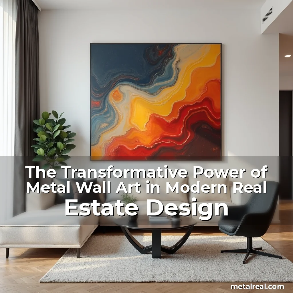
The Transformative Power of Metal Wall Art in Modern Real Estate Design
The Transformative Power of Metal Wall Art in Modern Real Estate Design Metal wall art is redefining interior aesthetics across luxury homes, commercial spaces, and investment properties worldwide. As real…

Mastering Custom Metal Artwork for Better Results
The Transformative Power of Custom Metal Art in Real Estate Development and Investment In an era where architectural differentiation is paramount, custom metal artwork has emerged as a powerful tool…
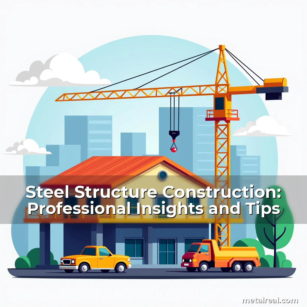
Steel Structure Construction: Professional Insights and Tips
The Strategic Advantages of Steel in Modern Real Estate Development In an era where sustainability and efficiency define architectural innovation, steel structure construction has emerged as a cornerstone of modern…
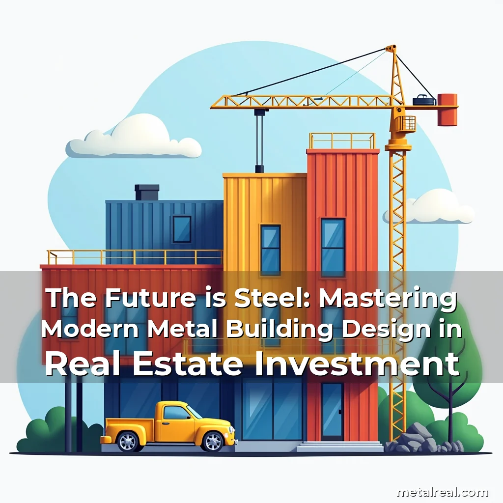
The Future is Steel: Mastering Modern Metal Building Design in Real Estate Investment
The Future is Steel: Mastering Modern Metal Building Design in Real Estate Investment In an era where sustainability meets innovation, metal building design has emerged as a cornerstone of modern…
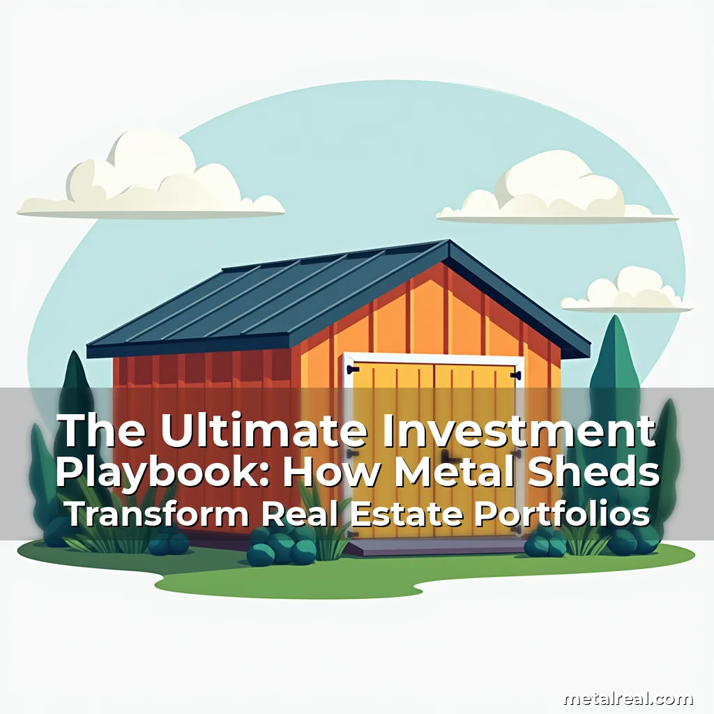
The Ultimate Investment Playbook: How Metal Sheds Transform Real Estate Portfolios
The Ultimate Investment Playbook: How Metal Sheds Transform Real Estate Portfolios In the high-stakes world of real estate investment, savvy professionals are constantly seeking innovative ways to enhance property value…
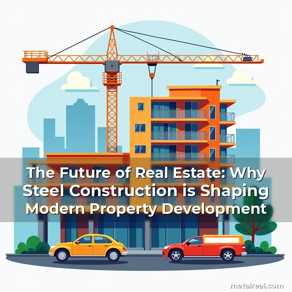
The Future of Real Estate: Why Steel Construction is Shaping Modern Property Development
The Future of Real Estate: Why Steel Construction is Shaping Modern Property Development In an era where sustainability, speed, and strength are paramount in real estate development, steel construction has…
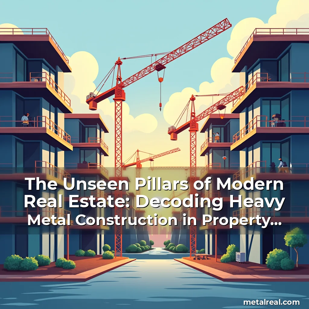
The Unseen Pillars of Modern Real Estate: Decoding Heavy Metal Construction in Property Development
The Unseen Pillars of Modern Real Estate: Decoding Heavy Metal Construction in Property Development In an era where skyscrapers pierce the clouds and urban landscapes evolve at breakneck speed, the…
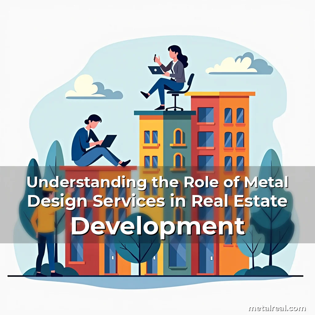
Understanding the Role of Metal Design Services in Real Estate Development
Revolutionizing Real Estate: How Custom Metal Design Elevates Property Value and Aesthetic Appeal Metal design services are reshaping the landscape of modern real estate development, offering solutions that blend functionality,…
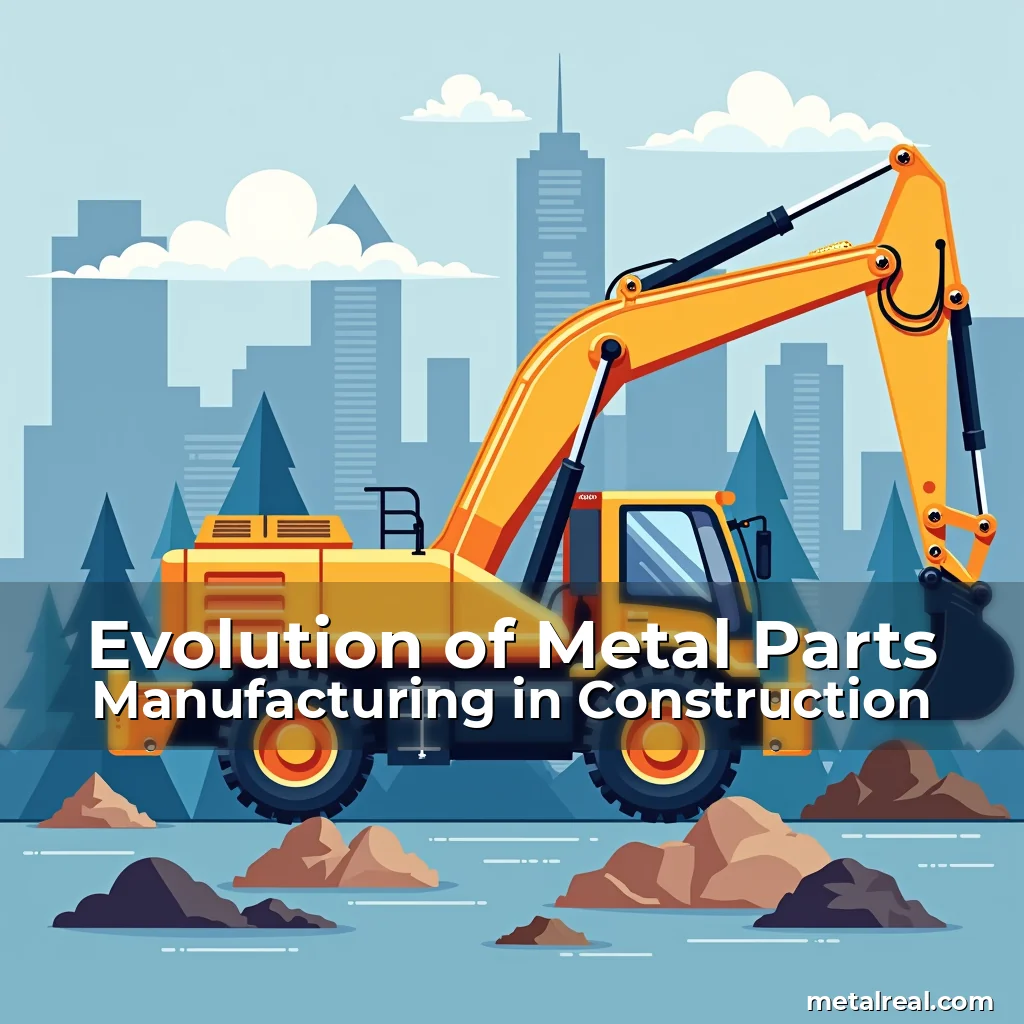
Evolution of Metal Parts Manufacturing in Construction
The Role of Precision Metal Fabrication in Modern Real Estate Development and Infrastructure Projects In an era where construction projects demand unprecedented levels of precision and durability, the role of…